(Hong Kong)


Product Summary
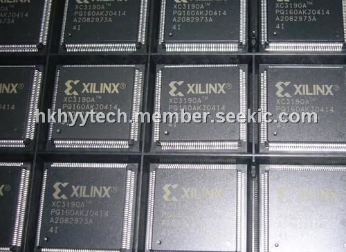
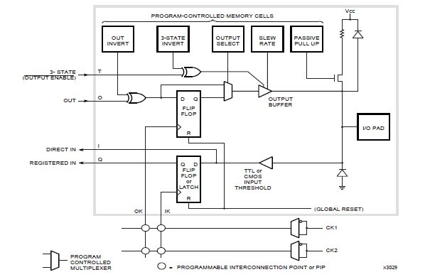
The XC3190A Field Programmable Gate Arrays (FPGAs) provide a group of high-performance, high-density, digital integrated circuits. Their regular, extendable, flexible, user-programmable array architecture is composed of a configuration program store plus three types of configurable elements: a perimeter of I/O Blocks (IOBs). The development system provides schematic capture and auto place-and-route for design entry. Logic and timing simulation, and in-circuit emulation are available as design verification alternatives. The design editor of XC3190A is used for interactive design optimization, and to compile the data pattern that represents the configuration program.
Parametrics
XC3190A absolute maximum ratings: (1)Supply voltage relative to GND, VCC: –0.5 to +7.0V; (2)Input voltage with respect to GND, VIN: –0.5 to VCC+0.5V; (3)Voltage applied to 3-state output, VTS: –0.5 to VCC +0.5 V; (4)Storage temperature (ambient), TSTG: –65 to +150℃; (5)Maximum soldering temperature (10 s @ 1/16 in.), TSOL: +260℃; (6)Junction temperature plastic, TJ: +125℃; (7)Junction temperature ceramic, TJ: +150℃.
Features
XC3190A features: (1)Complete line of four related Field Programmable Gate Array product families; (2)Ideal for a wide range of custom VLSI design tasks; (3)High-performance CMOS static memory technology; (4)Flexible FPGA architecture; (5)Unlimited reprogrammability; (6)Extensive packaging options; (7)Ready for volume production; (8)Complete Development System.
Diagrams
| Image | Part No | Mfg | Description |  |
Pricing (USD) |
Quantity | ||||||
|---|---|---|---|---|---|---|---|---|---|---|---|---|
 |
 XC3190A-3PC84C |
|
IC LOGIC CL ARRAY 9000GAT 84PLCC |
Data Sheet |
|
|
||||||
 |
XC3190A-3PQ160C |
|
IC LOGIC CL ARRAY 9000GAT 160PQF |
Data Sheet |
Negotiable |
|
||||||